
汽車電子產品的一個普遍要求是直接連接到配線裝置,必須能夠經得起電池電壓的短路。雖然殘酷,但這項規定對可靠性與安全來說是必要的。一個需要這種保護的例子是用于汽車內部產生間接噪聲的音頻放大器。雖然工作電壓為3.3或5v,低于電池電壓,但放大器必須能夠忍受滿電池電壓。還可以使用適合其他汽車電路中放大器的保護網絡 (圖1)。一個雙N溝道場效應管隔離從接線結點到另一端的高壓條件的放大器輸出。該場效應管,Q1A 和Q1B,通常情況下是開著的;齊納擊穿二極管D4及其偏置元件驅動場效應管的門限大約達到11V。雙二極管D3提供OR二極管連接到每個輸出的直流電壓,從而產生電壓控制分流調節器IC2的輸出。電路保護IC1,1.4W的AB類放大器適于為汽車電子提供聲音警告和指示。
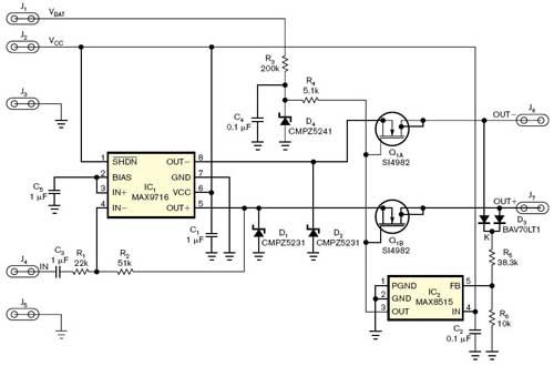
圖1 適合其他汽車電路中放大器的保護網絡
系統正常運行時,放大器輸出的直流分量是VCC的一半——VCC為5V的情況下是2.5V。11V的門限驅動全面提升了
場效應管,而分流調節器的輸出被關閉,因為它的反饋輸入,第5腳,低于內部門限0.6V。如果輸出超過5V,電流流經D3到R5/R6分壓,拉動反饋端到其門限之上。然后分流調節器的輸出拉著場效應管的柵極電壓從11V接近地,關掉場效應管來阻塞放大器的高電壓。場效應管很容易承受連續輸出電壓,當短路故障排除后,電路恢復正常運作。由于電路不能瞬間響應,齊納擊穿二極管D1 和D2在故障狀態開始時提供了保護。
圖2的波形顯示了一個操作電路。放大器的輸出之一(軌跡1)是一個偏置2.5V直流1kHz的正弦波。軌跡2是線束信號。它開始也是一個偏置為2.5V,1kHz的正弦波,但在200µs時,短接到一個18V電源上。 軌跡3是分流調節器的輸出,最初偏置是11V,但被拉到地來響應過壓狀態。軌跡4是線束的電流。起初為正弦波,該電流在響應過載電壓時降至零。

圖2 波形顯示了一個操作電路
圖1的元件在5V時工作達到最優化。對其他電壓值,可以調整的R5/R6的電阻值。分流調節器必須能夠起飽和作用,因此除了逃避輸出端外,還需要隔離電源管腳。該電路可以反復經受28V短路而不損壞。
英文全文:
Circuit guards amplifier outputs against overvoltage
An automotive-protection circuit withstands repeated insults of direct short circuits to the full battery voltage.
John Guy, Maxim Integrated Products, Sunnyvale, CA; Edited by Charles H Small and Fran Granville -- EDN, 7/5/2007
A universal requirement for automotive electronics is that any device with direct connections to the wiring harness must be able to withstand shorts to the battery voltage. Though brutal, this requirement is necessary for reliability and for safety. One example of the need for this protection is an audio amplifier that produces indicator noises in the automotive interior. Though operating from a voltage of 3.3 or 5V, which is lower than the battery voltage, the amplifier must be able to stand off the full battery voltage. You can also use a protection network appropriate for these amplifiers for other automotive circuits (Figure 1). A dual N-channel MOSFET disconnects the amplifier’s outputs from the wiring harness in response to a high-voltage condition on either output. The MOSFETs, Q1A and Q1B, are normally on; zener diode D4 and its bias components drive the MOSFETs’ gates to approximately 11V. Dual diode D3 provides a diode-OR connection to the dc voltage on each output, thereby producing a voltage that controls the output of shunt regulator IC2. The circuitry protects IC1, a 1.4W Class AB amplifier suitable for audible warnings and indications for the automotive electronics.
During normal operation, the amplifier outputs’ dc components are at one-half of the VCC supply—2.5V in this case, for which VCC is 5V. The 11V gate drive fully enhances the MOSFETs, and the shunt-regulator output is off
because its feedback input, Pin 5, is below its internal 0.6V threshold. If either output exceeds 5V, current flows through D3 into the R5/R6 divider, pulling the feedback terminal above its threshold. The shunt-regulator output then pulls the MOSFET-gate voltage from 11V almost to ground, which blocks high voltage from the amplifier by turning off the MOSFETs. The MOSFETs easily withstand the continuous output voltage, and the circuit returns to normal operation when you remove the short. Because the circuit does not respond instantaneously, zener diodes D1 and D2 provide protection at the beginning of a fault condition.
The waveforms of Figure 2 represent an operating circuit. One of the amplifier’s outputs (Trace 1) is a 1-kHz sine wave biased at a dc voltage of 2.5V. Trace 2 is the signal on the wire harness. It also starts as a 1-kHz sine wave biased at a 2.5V-dc voltage, but, at 200 µsec, it shorts to an 18V supply. Trace 3 is the shunt regulator’s output, initially biased at 11V but pulled to ground in response to the overvoltage condition. Trace 4 is current in the wire harness. Initially a sine wave, this current drops to zero in response to the overvoltage condition.
The components in Figure 1 optimize this circuit for 5V operation. For other voltages, you can adjust the R5/R6 resistor values. The shunt regulator must be able to function in saturation and, therefore, requires a separate supply pin in addition to the shunt output pin. The circuit repeatedly withstands 28V shorts without damage.